Free Download Electrical Diagram Software. P-n junctions are usually formed by joining up of p-type and n-type semiconductor materials.
photodiode diode symbol photodiodes terminals semiconductor diodes anode types working cathode electronics lik Its capability to turn off is due to the diversion of PNP collector current by the gate and thus breaking the regenerative feedback effect. Change MOSFET Envelope from Visible to Invisible, Modify MOSFET Channel from P-Type to N-Type, Modify MOSFET Type from Depletion to Enhancement, Modify the MOSFET Substrate Connection: None, Internal,
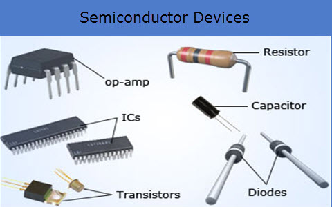
Semiconductor devices can be found as both discrete components devices as well as integrated circuits. Due to these capacitances, the transistor does not turn on or turn off instantly. It can also switch off much faster than a p-n junction diode. The resistivity of this drift region is dependent on the value of the base current. Its physical cross-sectional structural diagram and equivalent circuit diagram are presented in Figure27 to Figure29. Illustration. A fictitious diode anode is connected to the source and its cathode is connected to the drain.
diode semiconductor symbol characteristics theory types figure type electricalacademia This is called a delay time. The diode current flows for a reverse-recovery time (trr). & Conditions, License
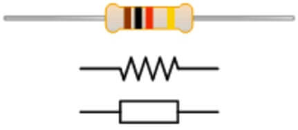
resistor symbol symbols resistors types variable different its applications powerpoint electrical Required fields are marked *. S-factor <1 large oscillatory overvoltage (snappy-recovery diode or fast-recovery diode). Can it be implemented in the practical circuit as it is. For high power, mesa construction is used where the inner layer is diffused and the two outer layers are alloyed on it. Tunnel diode, Varactor, Diac, Triac, Controlled switch, Controlled rectifier,
Standard Semiconductor Symbols For Electrical Schematic Diagrams, Visio A pure semiconductor is known as Intrinsic Semiconductor while an impure or doped semiconductor is known as Extrinsic Semiconductor. This total delay can be reduced by using a low-impedance drive circuit. Power n-p-n transistors are widely used in high-voltage and high-current applications which will be discussed later. Types, Applications, What Does SMT Mean in Electronics?
This is the power dissipation for when the diode is forward biased. document.getElementById( "ak_js_1" ).setAttribute( "value", ( new Date() ).getTime() ); Get great content that you love. switching operations. The two types of characteristics of a power diode are shown in Figure3 and Figure4.

Before the usage of semiconductor materials in electronic devices, vacuum tubes were used design of electronic components.
 eplan inductor capacitor
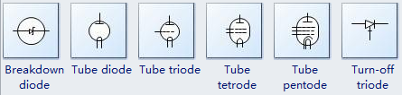
 It has no body diode as in the case of MOSFET but this can be seen as an advantage ofusing an external fast recovery diode for specific applications. But all these can be dialed back to the heart of modern electronics and its manufacturing: Semiconductor Devices. diode, tube triode, tube triode, tube pentode and turn-off triode. Due to NPNP structure instead of PNPN, anode acts as a reference for gate. Traditionally, group IV elements like Silicon (Si) and Germanium (Ge) are considered the Elemental Semiconductor Materials i.e.

As drain current has reached the constant value, the gate-to-source voltage is also constant as shown in the transfer characteristics of MOSFET in Figure20. In such cases, an external fast-recovery diode is connected in an antiparallel manner. The semiconductor symbols below show some graphic

Electrical Symbols Semiconductor | Electrical Drawing Software Symbol Of All Electronic Device In Pdf, Semiconductor Devices Symbol And Components, Symbol And Circuit Diagram Semiconductor Devices. diagrams. Thus, the switching characteristics of a power MOSFET depend on these internal capacitances and the internal impedance of the gate drive circuits.
symbols semiconductor electrical schematic diagrams circuit diagram semiconductors software edrawsoft Even this conductivity can be further controlled by external or internal factors like, TVS Diode (Transient Voltage Suppression Diode), VCSEL (Vertical Cavity Surface Emitting Laser), For more information on some of the above mentioned semiconductor devices, read . N-channel enhancement type MOSFET is more common due to the high mobility of electrons. The symbol for GTO is shown in Figure 42. leaving it at right angles and then bending back at right angles into the same

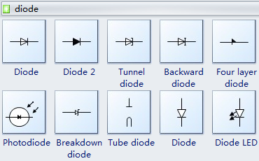
The vector stencils library "Semiconductor diodes" contains 24 symbols of semiconductor diodes for drawing electronic schematics and circuit diagrams.
diode symbols various zener vector shutterstock diodes electrical rectifier rectifiers schottky circuit rectify application royalty 
However, the drawback of this intrinsic layer is that it can addnoticeable resistance during forward-biased conditions, which means thatthe power diode could requirea proper cooling arrangement for handling large power dissipation. While a reverse bias junction has only a depletion capacitance in action. GTO can be turned on with the positive gate current pulse and turned off with the negative gate current pulse.
Some examples of three-terminal semiconductor devices include Bipolar transistor, IGBT, Field-effect transistor, Silicon-controlled rectifier, TRIAC, Thyristor, etc.
eplan inductor capacitor diodes diode Actually the design of GTO is made in such a way that the PNP current gain of GTO is reduced. Can you please explain, what is happening in the driver circuit of GTO. Electrical Symbols, Electrical Diagram Symbols, Electrical Symbols Semiconductor Diodes, Electrical Drawing Software and Electrical Symbols, Electrical Symbols, Electrical Schematic Symbols, Electrical Symbols Composite Assemblies, Electrical Symbols Logic Gate Diagram, Electrical Symbols Integrated Circuit, Semiconductor Devices Symbols Applications, All Semiconductor Devices Symbol And Real Images. metal comes in close contact with a semiconductor material. Hence, such a device, which allows the current to pass through them partially is called aSemiconductor Device.
diodes different types diode symbols schottky zener vs electrical electronic electronics led laser replace works active specialty recovery step various When a p-type MCT is in the forward-blocking state, it can be switched on by applying a negative pulse to its gate (with respect to anode). As compared to the p-n junction diode it has: Application: high-frequency instrumentation and switching power supplies. In simple words, Semiconductor devices are a type of electronic components that designed, developed and manufactured based on the Semiconductor materials like Silicon (Si), Germanium (Ge) and Gallium Arsenide (GaAs). In the case of the power diode, it almost increases linearly with the applied voltage as all the layers of P-I-N remain saturated with minority carriers under forwardbias. Ignoring the external factors like temperature and light for now, a process called Doping is generally performed to the semiconductor materials, where an impurity is introduced into its structure to change the structural as well as electrical properties. Traditional thyristors are designed without gate-controlled turn-off capability in which the thyristor can come from conducting state to a non-conducting state when only the anode current falls below the holding current. Since their use in late 1940s (or early 1950s), semiconductors became the main material in the manufacturing of electronics and its variants like optoelectronics and thermoelectronics. Assuming the drain-to-source voltage remains fixed. It has three terminals called collector, emitter, and gate.
types diode diodes electronic breakers physics semiconductor tutorvista earthlink webmail Switching characteristics of SCR are shown in Figure39. Underforward-bias conditions, the signal diode current can increaseexponentially and then increaselinearly. A forward-biased p-n junction has two capacitances named depletion layer capacitance and diffused capacitance. Therefore, there is only the movement of the majority carriers (electrons) and the turn-off delay caused by the recombination process is avoided.
diode symbol diodes types different fig Consider the device CPU, it consists of many numbers of transistors within it and these transistors contain the semiconductor material which allows the passage of current and all these are controlled by a switch.
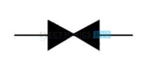
diode transistor difference between symbol semiconductor junction symbols circuitglobe Four layer diode and Photodiode symbols. The guard rings prevent the radius of the curvature of the depletion layer from becomingtoo narrow, which canincreasethe breakdown strength. For turning off the BJT, the polarity of the base voltage is reversed and thus the base current polarity will also be changed as shown in Figure26.
semiconductor diodes semiconductors diode outnews fish button. Thus, this can be used in inverter circuits for reactive loads without the need for excessive diode across a switch. The semiconductor examples include the following: These devices are widely used in many of the applications due to their reliability, compactness, low cost. Semiconductor Devices A semiconductor material is a device that allows the passage of electric current through it. In planar BJTs, the collector and emitter are on the same side of the wafer, while in power BJTs it is on opposite edges as shown in Figure 23. Even this conductivity can be further controlled by external or internal factors like electric field, magnetic field, light, temperature and mechanical distortion. current-controlled switch. BJTs use more silicon for the same drive performance. S-factor: the measure of the voltage transient that occurs during the time the diode recovers. For the time greater than t2, the drain current ID has reached its maximum constant value I. The labels on the Figure 4 graph are confusing/incorrect. Power loss across diode = vf* if(shown in Figure4c). Time Ta: Charges stored in the depletion layer removed. constructed of doped semiconductor material and may be used in amplifying or
For turn-off characteristics, assume that the MOSFET is already in the switched-on situation with a steady state. This time is known as the delay time (td) required to charge the junction capacitance of the base to the emitter to 0.7 V approx. Drain current in this duration remains at zero value. Thus, current from the drain to the source flows. As compared to the simple lateral channel MOSFET for low-power signals, power MOSFET has a different structure. It is controlled by the gate voltage.
transistors transistor npn type physics symbol bipolar junction semiconductor pnp definition introduction circuits devices electronic electronics radio 
Highly doped n spots in the anode p layer form a shorted emitter effect and ultimately decreases the current gain of GTO for lower current regeneration and also the reverse voltage blocking capability. Solid-state devices are completely made from a solid material and their flow of charges is confined within this solid material. This means the depletion layer has not punched through the lightly-doped n-layer. There are several devices in the MCTs family but the p-channel is commonly discussed. If the thickness of the lightly doped "I" layer (n-layer) is greater than the depletion layer width at the breakdown, this creates anon-punch through power diode. The Semiconductor symbols are smart, industrial standard and vector-based for electrical schematic
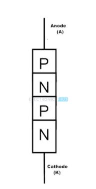
There are also a few four-terminal semiconductors like Optocoupler (Photocoupler) and Hall-effect Sensor. Its representation is shown in Figure18. The structure of the thyristor can be split into two sections: NPN and PNP transistors for simple analysis purposes as shown in Figure36. Additionally, if the thickness of the "I" layer is less than thedepletion layer width at the breakdown, this becomes the punch through the power diode. That means this BJT acts in a cut-off state. They are used in the designing of logic gates and digital circuits.
eplan inductor capacitor 
Before going in to the discussion about different types of Semiconductor Device, it is essential to have an idea about what a semiconductor is.
Now, if we will increase the gate-to-source voltage, the drain current will also increase. IGBT combines the physics of both BJTs and power MOSFETs to gain the advantages of both worlds. The BJT is a three-layer and two-junction NPN or PNP semiconductor device as given in Figures 22(a) and (b). But more width of the n-base indicates a slow response time for switching. Basics of Surface Mount, Classification and Different Types of Transistors | BJT,, Introduction to MOSFET | Enhancement, Depletion, Amplifier,. There is a delay from t0 to t1 due to the charging of input capacitance up to its threshold voltage VTH. No ads or spams, we promise. Semiconductor devices supply themselves in integrating into complex and are readily manufacturable into microelectronic circuits. =). It is the time between the instant forward diode current becoming zero and the instant reverse-recovery current decays to 25% of its reverse maximum value. Simply speaking Semiconductors are materials that are neither conductors nor insulators. The gate drive circuitry with switching characteristics is given in Figure43 and Figure 44. It has a high input impedance like a power MOSFET and has low on-state power loss as in the case of BJT. These are current-voltage characteristics curves. Its switching characteristic is also shown in Figure33. Another feature is to coatthe SiO2 layer to help limit the electric field at the surface of the power diode. But just like any other devices, it needs to be protected against transient voltages and current spikes with the help of suitable snubbers. Overall switching speed of GTO is faster than thyristor (SCR) but voltage drop of GTO is larger. ElectricalElectronicsEmbeddedPowerRoboticsARMIOT, Mini projectsMicrocontrollerArduinoSolarFree circuitsHome AutomationSeminar TopicsElectronicsQuestions, CapacitorsResistorsFiltersDiodesTransistorsAmplifiersIO DevicesThyristorsDC CircuitsNumber System, Speaking in terms of electrical conductivity with units of , In simple words, Semiconductor devices are a type of, As mentioned earlier, the electrical conductivity of semiconductor materials lies between that of conductors and insulators. Its schematic diagram and equivalent circuit is given in Figure45 and Figure46.
There is no even secondary breakdown and not have long switching time as in the case of BJT. In our electrical diagram
This time is called rise time, required to turn on the transistor. symbol. NPNP structure is represented by NPN transistor Q1 and a PNP transistor Q2 in the equivalent circuit.
symbols diode diodes types different symbol varactor electrical explained electronic characteristics electronics circuits physics names circuit schematic its various facts But in cases where it is connected externally, the symbol will change as shown in the n-channel enhancement type MOSFET in Figure9. Thus, in the case of IGBTs and MOSFETs, the drive circuit must be capable to charge and discharge the internal capacitances. This is called threshold voltage. The symbol of the thyristor is given in Figure35.

Usually metals have good electrical conductivity and you can find Copper or Aluminium in your homes electrical wiring. These devices are said to be neither good insulators nor good conductors, hence the name Semi Conductors. Basic circuit diagram and output characteristics of an n-channel enhancement power MOSFET with load connected are in Figure11 and Figure12 respectively. Besides the output characteristics curves, transfer characteristics of power MOSFET are also shown in Figure14. Electrical Symbols Semiconductor | Electrical Symbols All Examples Of Semiconductor Devices And Symbols, Different Types Of Symbols Semiconductor Devices, Symbols Characateristic Of Semiconductor Devices. Resources, EdrawMax
eplan logic constraint ecad mcad propagation integration inductor How to draw electrical
Glass, wood and paper are good examples of Insulators. As the source is connected to both base and emitter of this parasitic BJT, the emitter, and base of the BJT are short-circuited. Similarly, if the holes are increased, it is known as p-type semiconductor. This means thata high value of current can produceresults in avoltage drop that masks the exponential part of the curve. The static characteristic obtained from the circuit given in Figure37 is drawn in Figure38.
mosfet fet kb6nu schematic junction